|
|
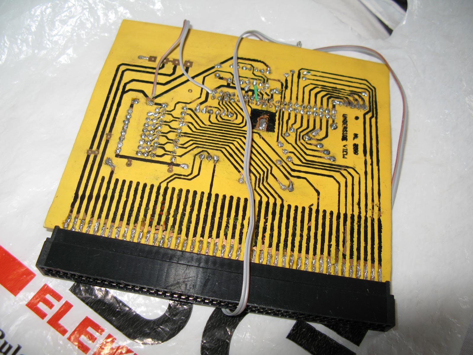
| A500IDE bottom view | ||
 |
||
| Previous Image | Next Image | ||
|
Description: Its the A500IDE bottom view. I used HP4L laser printer for making this PCB. IIRC it was the first (and only so far) PCB I ever 'etched' so its ugly.. At the time I didn't realize you're supposed to cover as much of copper as possible, so etching took a lot of time and acid.. heh Toner from printer is still there, as insulation and protection from oxidation. (I would use plastic spray now that I have it, but its hard to remove the toner) Picture Stats: Views: 1700 Filesize: 291.47kB Height: 768 Width: 1024 Posted by: orange at May 08, 2008, 08:26:19 AM Image Linking Codes
|
||
| 0 Members and 1 Guest are viewing this picture. |
| Tension Posts:2034 | February 18, 2009, 01:52:42 AM Impressive!!! |